
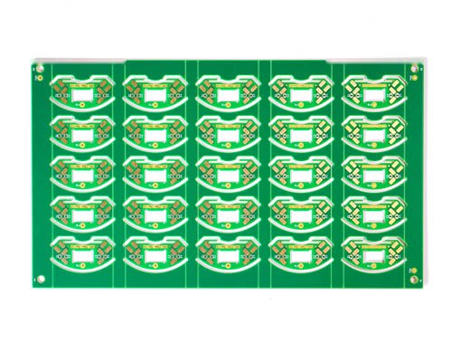
Single-sided
Simple single-layer FR4 boards.
FR4 PCB
1–32 layer FR4, HDI, heavy copper, high-Tg, RF and rigid-flex constructions with finishes and impedance control as specified.
01 Board types
Product families migrated from fabrication capability set.
Simple single-layer FR4 boards.
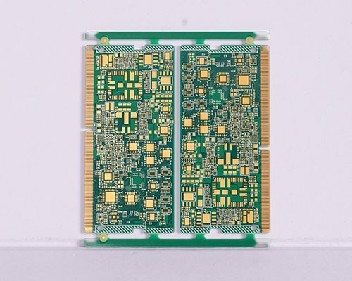
Dense routing through 32 layers.
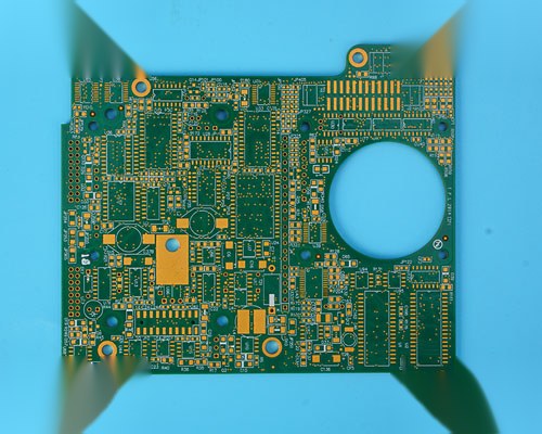
Microvias and fine pitch (3/3 mil class).
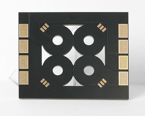
Outer/inner copper up to 30 oz class.
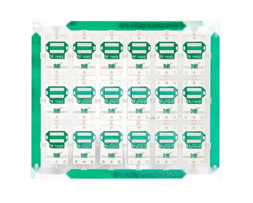
RF and high-frequency laminates.
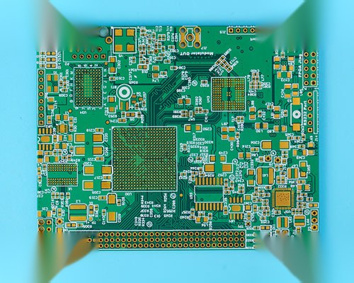
Tg > 130 / 150 / 170 / 180.
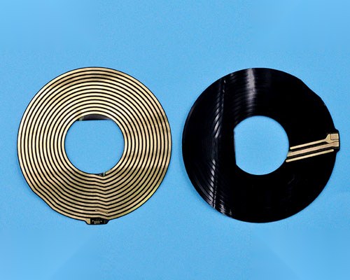
Down to 0.15 mm board thickness.
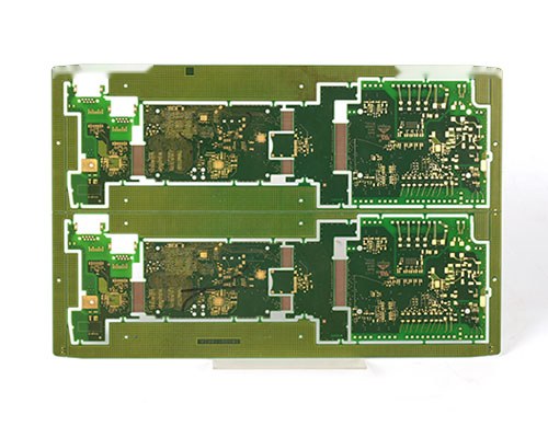
Semi rigid-flex constructions.
02 Capabilities
| Item | Capabilities |
|---|---|
| Layer count | 1 – 32 layers |
| Max board dimension | 24 × 24" (610 × 610 mm) |
| Min board thickness | 0.15 mm |
| Max board thickness | 6.0 – 8.0 mm |
| Copper thickness | Outer 1–30 oz; inner 0.5–30 oz |
| Min line / space | Normal 4/4 mil (0.10 mm); HDI 3/3 mil (0.076 mm) |
| Min hole diameter | Normal 8 mil (0.20 mm); HDI 4 mil (0.10 mm) |
| Min punch hole dia | 0.1" (2.5 mm) |
| Min hole spacing | 12 mil (0.3 mm) |
| Min PAD ring (single) | 3 mil (0.075 mm) |
| PTH wall thickness | Normal 0.59 mil (15 µm); HDI 0.48 mil (12 µm) |
| Min solder PAD dia | Normal 14 mil (0.35 mm); HDI 10 mil (0.25 mm) |
| Min solder mask bridge | Normal 8 mil (0.2 mm); HDI 6 mil (0.15 mm) |
| Min BGA PAD margin | 5 mil (0.125 mm) |
| PTH / NPTH dia tolerance | PTH ±3 mil (0.075 mm); NPTH ±2 mil (0.05 mm) |
| Hole position deviation | ±2 mil (0.05 mm) |
| Outline tolerance | CNC ±6 mil; die punch ±4 mil; precision die ±2 mil |
| Impedance controlled | >50 Ω: ±10%; ≤50 Ω: ±5 Ω |
| Max aspect ratio | 8:1 |
| Surface treatment | ENIG, flash gold, hard gold finger, gold plating, ENEPIG, ENIPIG, HAL, HASL (LF), OSP, immersion silver, immersion tin |
| Solder mask color | Green / white / black / yellow / blue / red |
03 Materials
| Item | Attribute |
|---|---|
| Brand | KB / SYL / Nanya / Isola / Nelco / Rogers / Taconic / Arlon / Hitachi / Panasonic / ITEQ |
| Material type | FR4 / FR-5 / CEM-1 / CEM-3 / FR1 |
| Thickness | 0.10 – ≥2.0 mm (standard steps) |
| Tg value | > 130 / 150 / 170 / 180 |
| Halogen free | Yes (optional) |
| RoHS | Yes |
| Flammability | 94V-0 |
| Thermal conductivity | 0.30 – 0.45 W/m·K |
| Dielectric strength | > 1.3 kV/mm |
| Wrap & twist | ≤ 0.75% |
| Thermal stress | 3 × 10 s @ 280 °C |
04 Lead time
| Layers | Normal | Expedited |
|---|---|---|
| 1 layer | 3 – 4 days | 24 hours |
| 2 layers | 4 – 6 days | 24 hours |
| 4 layers | 8 – 10 days | 48 hours |
| 6 layers | 8 – 10 days | 72 hours |
| 8 layers | 10 – 14 days | 72 – 96 hours |
| 10 layers | 14 – 18 days | 120 – 168 hours |
| HDI (1+N+1 / 2+N+2) | 2.5 – 3.5 weeks | On review |
| Layers | Normal | Expedited |
|---|---|---|
| 1 layer | 4 – 6 days | 2 – 3 days |
| 2 layers | 5 – 8 days | 2 – 3 days |
| 4 layers | 8 – 12 days | 3 – 5 days |
| 6 layers | 8 – 12 days | 4 – 6 days |
| 8 layers | 12 – 16 days | 6 – 8 days |
| 10 layers | 18 – 20 days | On review |
| HDI (1+N+1 / 2+N+2) | 3 – 4 weeks | On review |
Lead times are typical envelopes and depend on stack-up, finish and capacity at quote time.
CTA Get a quote
Include layer count, copper weight, finish, quantity — attach Gerbers or ZIP.