
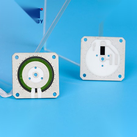
Thick film
Single–double sided, up to 4L.
Ceramic PCB
Alumina, AlN, ZTA and Si3N4 substrates with DPC, DBC, AMB, thick film, LTCC and HTCC process families.
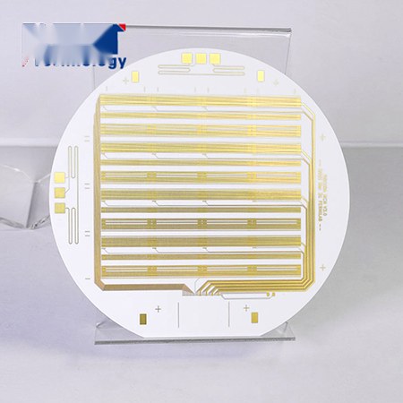
01 Process families
Process family is selected by thermal, RF and mechanical need.
Single–double sided, up to 4L.
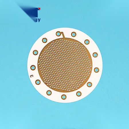
Fine features on ceramic substrates.
Direct plated copper, single–double sided.
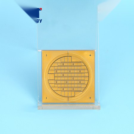
Direct bonded copper for power thermal paths.
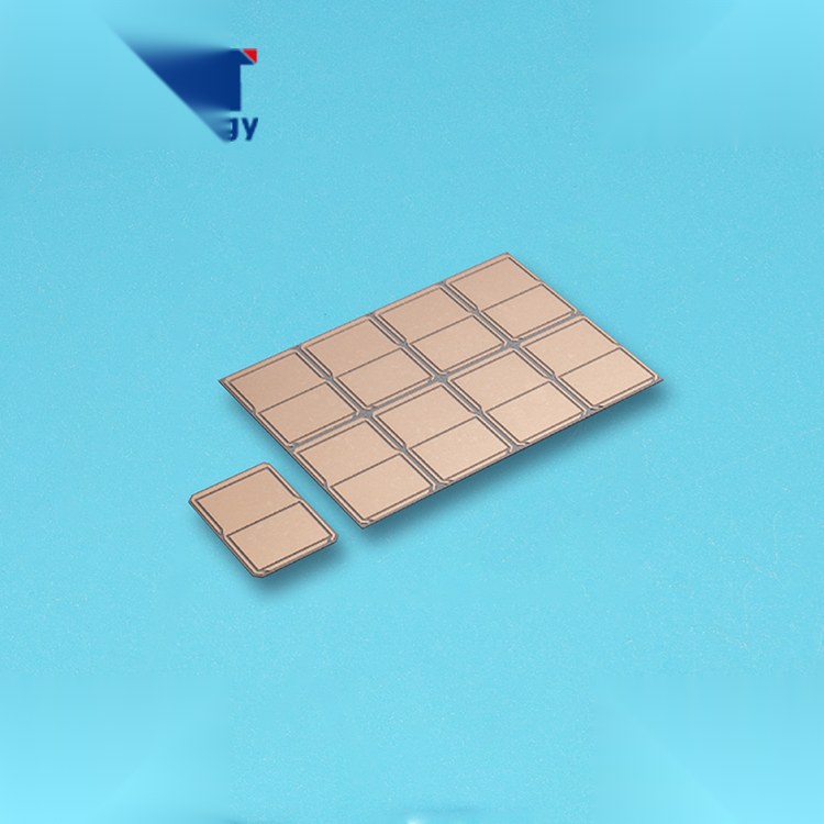
Active metal brazed ceramic boards.
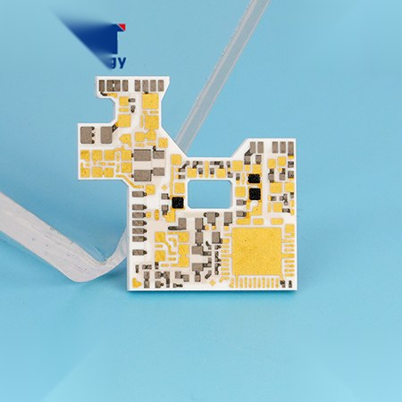
Low-temp co-fired; general to 6L, special to 14L.
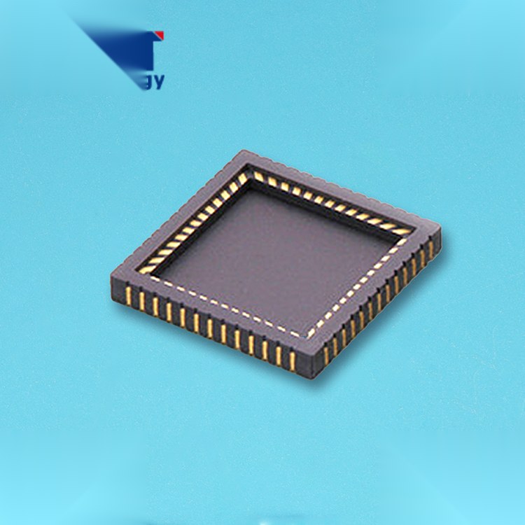
High-temp co-fired multilayer ceramic.
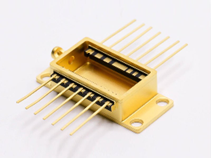
Package and carrier constructions.
02 Capabilities
Migrated manufacturing envelope — confirm final limits against your drawings.
| Item | General parameter | Special process |
|---|---|---|
| Al2O3 | High insulation, chemical and high-temp resistance | Glass, quartz, sapphire, 99% / 92% Al2O3 (black) |
| AlN | Excellent thermal conductivity, low CTE, high-temp | Glass, quartz, sapphire, 99% / 92% Al2O3 (black) |
| ZTA | Insulation performance and high-temp stability | Glass, quartz, sapphire, 99% / 92% Al2O3 (black) |
| Si3N4 | High strength, hardness, thermal conductivity, low dielectric loss | Glass, quartz, sapphire, 99% / 92% Al2O3 (black) |
| Conductor (LTCC/HTCC) | Tungsten, Au, Au&Pd, Au&Pb, Ag, Ag&Pd, Ag&Pb | Glass, quartz, sapphire, 99% / 92% Al2O3 (black) |
| DPC | Single – double sided | — |
| DBC | Single – double sided | — |
| AMB | Single – double sided | — |
| Thick film | Single – double sided, 4L | — |
| LTCC | Single – double sided, 4L, 6L | 6L – 14L |
| HTCC | Single – double sided, 4L, 6L | — |
| Inner layer | — | — |
| Outer layer | 1 oz – 3 oz (DPC) | 3 oz – 12 oz (DBC / AMB) |
| Max. dimension | 130 × 180 mm | Larger on evaluation |
| Min. dimension | 2 × 2 mm | Shipped in panel |
| Substrate thickness | Al2O3/AlN: 0.38 / 0.635 / 1.0 mm; Si3N4: 0.25 / 0.32 mm | > 1.5 mm |
| OSP | 0.2 – 0.5 µm | — |
| ENIG | Au 1–3 µ"; Ni 120–320 µ" | — |
| Immersion silver | 6 – 12 µ" | — |
| Immersion tin | ≥ 1 µm | — |
| ENEPIG | Au 2 µ", Pd 1 µ", Ni 100 µ" | — |
| Hard gold | Au 5–30 µ"; Ni 120–200 µ" | — |
| Min. PTH | 0.05 mm | — |
| Min. NPTH | 0.05 mm | — |
| Max. aspect ratio (PTH) | 5:1 | — |
| NPTH tolerance | ±0.05 mm | — |
| PTH tolerance | ±0.05 mm | — |
| Dielectric / mask | Glass glaze, medium, solder mask ink | — |
| Solder mask color | White, black, green | Mixed color |
| Silkscreen color | White, black | Mixed color |
| Silkscreen size | Line width ≥ 0.13 mm; height ≥ 0.8 mm | — |
| Solder mask thickness | ≥ 20 µm | — |
| Solder mask bridge | ≥ 0.15 mm | 0.1 mm |
| Outline tolerance | ±0.05 mm | ±0.1 mm |
| Min. tolerance (PTH) | ±0.05 mm | ±0.1 mm |
| Min. tolerance (NPTH) | ±0.05 mm | ±0.1 mm |
| Min. circuit to board edge | 0.2 mm | 0.15 mm |
| Finished thickness | 0.2 – 2.0 mm | ≥ 2.0 mm |
| Min. finished board thickness tol. | <1.0 mm: ±0.1 mm; >1.0 mm: ±10% | — |
Values describe a typical manufacturing envelope. Final capability is confirmed against your Gerbers and stack-up.
CTA Get a quote
Include process family, substrate and size — attach Gerbers, PDF or ZIP.